Дизайн платы pcb Smart
- Категории: Двухсторонняя печатная плата >>>
- Поставщик: Shenzhen,Anlida,Electronics,Technology,Co.,Ltd.

Поделиться:
Описание и отзывы
Характеристики
Product Description
Smart home product pcb board design
Design show


Design-parameters:

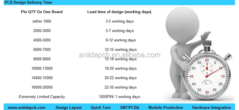
Design Delivery Time:
Design completed:
| Design completed data | |||||
| PCB Layout File | YES | Manufacturing File | YES | DXF File | YES |
| PAST File | YES | Silk File | YES | XY coordinates File | YES |
Mail Content Display :
Attached you can find the fabrication files for the ABCD single board, all the fabrication and assembly process as per the following files.The design files shall be deleted within 3 days after fabrication,so please back up the files,thank you !
--ABCD_PCB.ZIP → the pcb design files(.brd,.pcb)
--ABCD_CAM.ZIP → the file for pcb manufacturing
--ABCD_ASM.ZIP → the assembly files for pcb welding
--ABCD_SMD.ZIP → the SMT files for the SMT manufacturing
--ABCD_DXF.ZIP → the structure files for comfirming structure
--ABCD_SILK.ZIP → the silkscreen files for reference use of the assembly factory
Any questions ,please contact me ,thank you !
Hope we have a nice cooperation!
flow diagram:

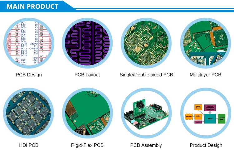
Main Product
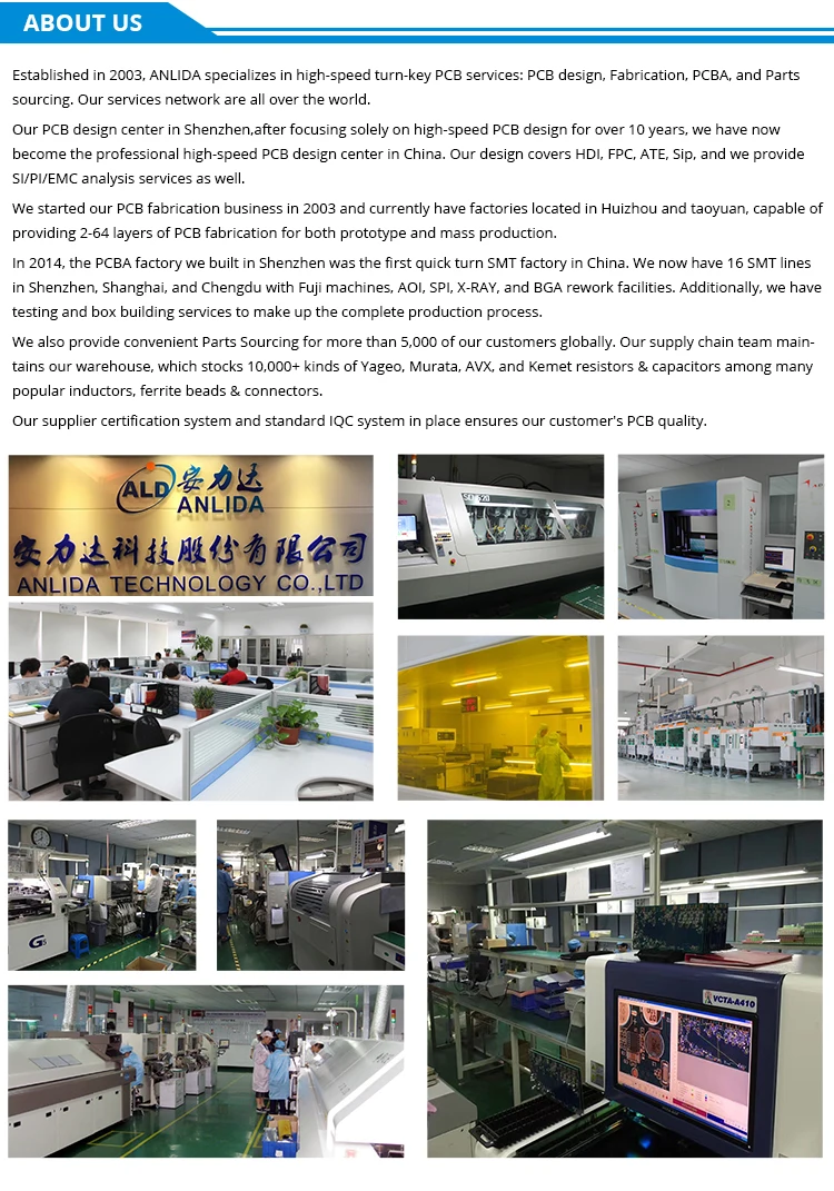
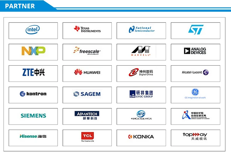
Company Information
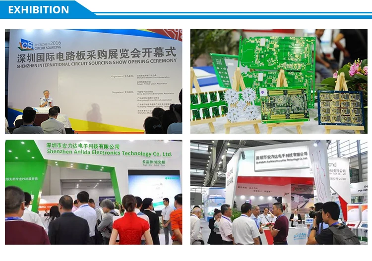
Exhibition
OUR Advantages


FAQ

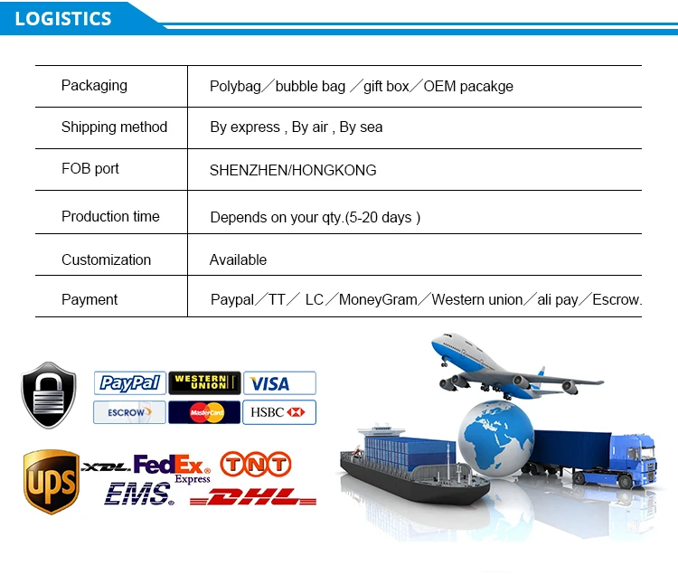
LOGISTICS
Contact US

Похожие товары


Новинки - Розница