Плата HASL ENIG FR4 толщиной 1 6 мм толщина меди унция зеленый цвет белый шелкография проверка функций программирования
- Категории: Жесткая печатная плата >>>
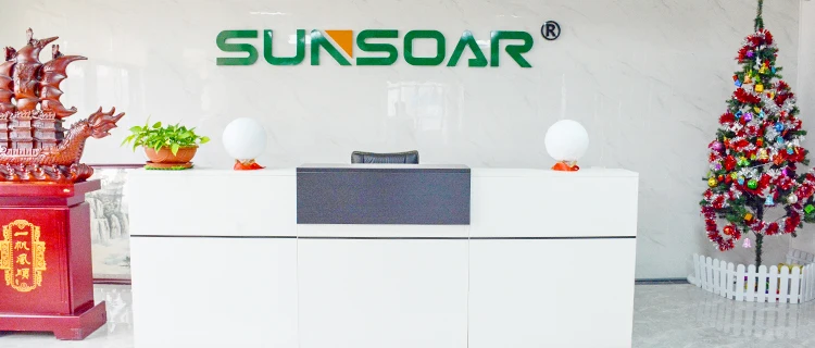
- Поставщик: Shenzhen,Sunosoar,Tech,Co.,Ltd.

Поделиться:
Описание и отзывы
Характеристики
COMPANY PROFILE
Shenzhen Sunsoar Tech Co.,LTD is a professional manufacturer of PCB(printed circuit board) and PCB assembly factory, located in Shenzhen, China.
Sunsoar was established by a group of young engineers and sales, started PCB career at 2008, after 10 years of hard working and keep developing, now we have PCB department and SMT(PCB assembly) department, our production ability is 10000㎡/month.
Sunsoar's products are widely applied in electronic deivces and household appliances, such as telecom, automobile , computer, medical equipment and consumer electronics. Our products and service is well accepted abroad, especially in Europe and America, Australia, Middle East, Southeast Asia.


Product Process
Sunsoar has invested in the best equipment, environment and staff training.
We have has been committed to R&D The professioonal high-precision and special material PCB and has the ability to make 4-28 layers high-precision impedance, multi-layer blind-layer hole, high Tg, Al base, Copper base and ceramic base PCB, 1-6 layer FPC, Etc.
The company takes ISO9000 Standardization managemeng and have certified UL,RoHS international certification.

COMPANY PROFILE
Shenzhen Sunsoar Tech Co.,Ltd
With experience over 8 years of OEM printed circuit board(PCB) and PCB assembly manufacturing, along with excellent quality, professional services and competitive prices, Sunsoar has won many customers' trust and support.
Shenzhen Sunsoar Tech Co.,Ltd is a professional manufacturer of printed circuit board and PCB assembly, with our own engineer team, SMT machine, DIP manual line and independent plants.
Production Process
Sunsoar has invested and keep expanding the best equipment, staff training and overseas clients.
We are being committed as R&D professional high-precision and special material PCB and capable to produce 4-28 layers high-precision impedance, multi-layers and blind-layer hole, FR4, high Tg, Aluminum board, Copper board and ceramic board PCB, 1-6 layers FPC, Etc.
Sunsoar is authorized by ISO9000 Standardization management, and meanwhile with UL,RoHS international certification.
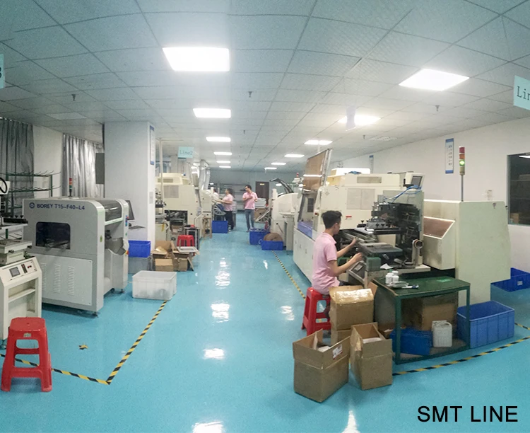
AOI Testing
1 Line Multi-Function Placement Machine
2-Wire Panasonic High-Speed Placement Machine
OUR SERVICE
1. Professional engineer team is standby to provide PCB design service and advice.
2. Check and evoluate your projects based on your files such as Gerber and BOM, including components source and professional advices.
3. The total cost could be quoted within 24 hours, no matter prototype or batch order.
4. From SMT/solder/assembly/DIP manual work till function test, from beginning to good working products received.
5. Easy and convenient delivery from DHL to local post, we can arrange delivery for you.
On-stop service products
We have built a wonderful and effective procedure from PCB design, PCB manufacture, SMT/assembly/manual DIP till function test, one-stop source from electronic suppliers. We believe we will be your best supplier and we will move forward together!
CAD
Layout
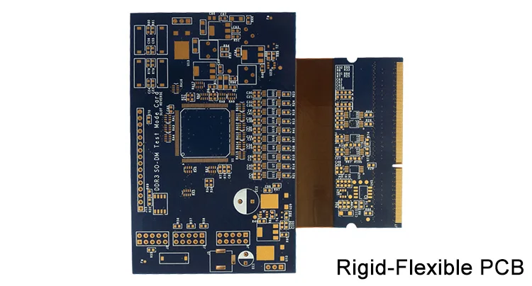
Rigid PCB
Quick turn PCB
FPC
FPC Fabrication
SMT
PCB Assembly
PRODUCT DESCRIPTION
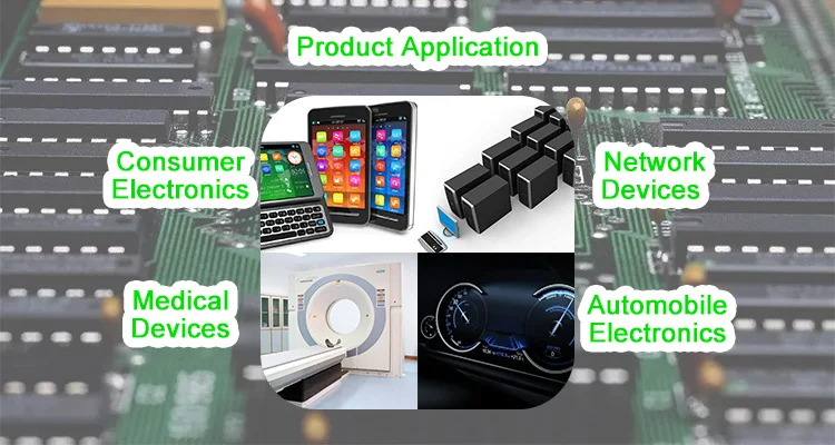
Product Application
Sunsoar Tech supplies PCB and PCBA OEM/Customize service, produce based on specification, Gerber and BOM.
Our products are widely applied from telecome device to medical equipments, from agriculture machine to industries as diverse as Medical devices through to consumer electronice, automobile electronics computer&network devices and communiction apparatus etc.

ITEM | TECHNICAL DATA | ITEM | TECHNICAL DATA |
Layers | 2-30(layers) | Min Board Thickness | 4layers:0.40mm/16mil |
Max Board Size | 250x650mm | 6layers:0.80mm/32mil | |
Min Line Width | 0.10mm/4mil | 8layers:1.00mm/40mil | |
Min Line Space | 0.10mm/4mil | 10layers:1.20mm/48mil | |
Min Hole Size | 0.20mm/8mil | Insulation Resistance | 1E+12Ω(Normal) |
PTH Wall Thickness | 0.020mm/0.8mil | Aspect Ratio | 10:1 |
PTH Dia Tolerance | ±0.05mm/±2mil | Thermal Shock | 288℃/3x10Sec@288℃ |
NPTH Hole Dia Tolerance | ±0.025mm/±1mil | Warp and Twist | ≤0.7% |
Hole Position Deviation | ±0.05mm/±2mil | Electric Strength | >1.3KV/mm |
Outline Tolerance | ±0.1mm/±4mil | Peel Strength | 1.4N/mm |
S/M Pitch | 0.08mm/3mil | Solder Mask Abrasion | >6H |
Flammability | 94V-0 | Impedance Control | ±5% |


Our One-Stop Service
1, PCB drawing/design according to your schematic diagram.
2, PCB fabrication.
3, PCB manufacturing.
4, Component sourcing.
5, PCB Assembly - SMT, DIP, Solder, Reflow Solder, Manual work.
6, PCBA function test.
PRODUCT DESCRIPTION
PCB Capacility
This form demonstrates specification and requirement of multilayer PCB
ITEM | TECHNICAL DATA | ITEM | TECHNICAL DATA |
Layers | 2-30(layers) | Min Board Thickness | 4layers:0.40mm/16mil |
Max Board Size | 250x650mm | 6layers:0.80mm/32mil | |
Min Line Width | 0.10mm/4mil | 8layers:1.00mm/40mil | |
Min Line Space | 0.10mm/4mil | 10layers:1.20mm/48mil | |
Min Hole Size | 0.20mm/8mil | Insulation Resistance | 1E+12Ω(Normal) |
PTH Wall Thickness | 0.020mm/0.8mil | Aspect Ratio | 10:1 |
PTH Dia Tolerance | ±0.05mm/±2mil | Thermal Shock | 288℃/3x10Sec@288℃ |
NPTH Hole Dia Tolerance | ±0.025mm/±1mil | Warp and Twist | ≤0.7% |
Hole Position Deviation | ±0.05mm/±2mil | Electric Strength | >1.3KV/mm |
Outline Tolerance | ±0.1mm/±4mil | Peel Strength | 1.4N/mm |
S/M Pitch | 0.08mm/3mil | Solder Mask Abrasion | >6H |
Flammability | 94V-0 | Impedance Control | ±5% |
Product Application
Our products are widely applied in electronic devices and household appliances, such as telecom, autoparts, automoblie electronics, computers, medical equipments and consumer electronics.
Product Display
Since established by a group of young engineer and sales in 2008, Sunsoar keeps developing and expanding, it is being committed as R&D professional high-precision and special material PCB and capable to make 4-28 layers high-precision impedance, multi-layer blind-layer hole, high Tg,Albase, Copper base and ceramic PCB,1-6 layers FPC , Etc.
The company takes ISO9000 Standardization managemeng and have certified UL,RoHS international certification.WE has been effort to build PCB design + PCB manufacture+SMT Assembly one-stop sourece of integrated electronic suppiser.

Rigid PCB Quick turn delivery
1-20 layer of hign-precision impedance boards,blind&
buried boards,HDI board.
Base materials:FR4,FR4 High TG(TG150,TG170).

PCBA Welcome OEM
Electronic Components sourcing.PCB Assemblies,PCBA Assemblies,PCBA function test OEM&ODM are welcomed,No MOQ requirements
PACKING&DELIVERY

Inquiry
1. PCB: please provide Gerber file with order quantity to us, also with specification such as material, layers, board thickness, copper thickness, surface finishing(HASL/ENIG), and solder mask with silkscreen, so we can check and quote accurately.
2. PCBA: please provide Gerder part as 1 and BOM.( BOM: Bill of Material, normally for details of components, such as designator, value, comments, package/footprint, brands, etc.)
3. PCB/PCBA clone service: please provide us the details of PCB such as dimension. clear photos for components and silksceen, IC's code/part number is most important. Sample would be better.
Quotation
1. We need details and requirement to confirm PCB and components.
2. PCB quotation would be offered within 24 hours.
3. PCBA quotation will be offered within 2 working day.
Delivery Time
Bare PCB
LAYER | PROTOTYPE | MASS PRODUCTION (above 30 m2) | ||
Quick Turn | Usual Time | |||
2 | 24 hours | 3-4 days | 8-10 days | |
4 | 48 hours | 5-6 days | 10-12 days | |
6 | 72 hours | 6-8 days | 12-14 days | |
8 | 72 hours | 8-10 days | 16-18 days | |
10 | 96 hours | 12-12 days | 18-20 days | |
....... | ....... | ....... | ....... | |
PCB Assembly
Order conditions | Standard Delivery Date | The Fastest Delivery Date |
prototype(<20 pcs) | 2 days | 8 hours |
small volum(20-100pcs) | 3 days | 3 days |
medium volum(100-1000pcs) | 6 days | 24 hours |
mass production(>1000pcs) | Depends on BOM | Depends on BOM |
Похожие товары


Новинки - Розница