

Гексагональный нитрид бора для косметики
US $36.20-$37.10

Поделиться:


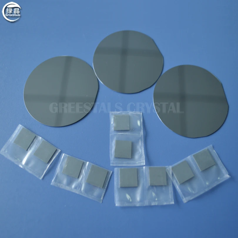
Ge can be used to make materials such as semiconductor devices, infrared optical devices, and solar cell substrates.
Main Property Parameters | |||
Growth Method | Czochralski | ||
Crystal System | Cubic | ||
Crystal Lattice Constant | a=5.65754 Å | ||
Density | 5.323g/cm3 | ||
Melt Point | 937.4℃ | ||
Doping Element | no | Sb | Ga |
Type | / | N | P |
Resistivity | >35Ωcm | 0.01~35 Ωcm | 0.05~35 Ωcm |
EPD | <4×10³/cm2 | <4×10³/cm2 | <4×10³/cm2 |
Dimension(mm) | 10x3,10x5,10x10,15x15,,20x15,20x20, | ||
Dia50.8 mm ,dia76.2mm, Dia100 mm | |||
Thickness | 0.5mm,1.0mm | ||
Polishing | One side or two sides | ||
Crystal Orientation | <100>,<110>,<111>,±0.5º | ||
Crystal Plane Orientation Accuracy | ±0.5° | ||
Edge Orientation Accuracy | 2°(special requirements <1°) | ||
Bevel Wafer | According to specific requirements, wafers with edge-oriented crystal planes inclined at a specific angle (inclination angle 1°-45°) can be processed. | ||
Surface Roughness | ≤5Å(5µm×5µm) | ||
Packaging | Clean bag (100), Super clean room (1000) | ||