


FR4 Double Sided PCB computer mainboard
- Категории: Rigid PCB >>>
- Поставщик: Shenzhen,Fly,Pcb,Electronic,Co.,Ltd.

Поделиться:
Описание и отзывы
Характеристики
Product Description
FR4 Double Sided PCB board for computer use
* Customized circuit board.
* 100% testing.
* Accept sample and bulk order.
| \t | \t |
| \t | \t |
| \t | \t |
| \t | \t |
| \t | \t |
| \t | \t |
| \t | \t |
| \t | \t |
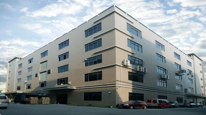
Company Profile
Fly PCB Electronic Co.,Ltd. is a manufacturer specializing in the research & development, manufacture and marketing of PCB boards. We have had about 300 workers and 15 R&D technicians since our company was established in Shenzhen City of Guangdong Province in 2003. Covering an area of 8,000 square meters, our workshops are equipped with about 60 binding machines.
Our Advantages
20 years experience
Professional PCB factory
Quality control
100% testing before ship
Sincerely service
To Meet the customer requires
FAQ
Q1. If you don't have any file, how can you get the price?
Tell me your quantity and model number, and PCB board size. We can make estimate price for you.
Or sample if you could provide.
Q2.Can I have a sample to test?
A:Yes.
Q3.What is the lead time?
A:PCB board:Samples need 7 working days,mass production needs 10-15working days, according to the order volume.
B:PCBA: Samples 15working days. mass production 20-25working days, according to the order volume.
Q4.Do you have MOQ limit?
A:Even 1 pcs,we care.
Q5.Can you offer the best price for us?
A:Yes,we are specialized PCB AND PCBA manufacturer for 20years directly,we can offer lower price than any trading company.
Q6.How do you ship the goods and how long does it take arrival?
A:Usually ship by DHL,UPS,FedEx and TNT.It takes 3-5days to arrive.
Q7.What are the payment terms?
A: Paypal,Western Union and T/T Bank is acceptable.
Q8.Can we visit your factory?
A:Yes,welcome to visit our factory anytime. We will show you our factory and production line.
Package
PRODUCTION PROCESS
Production line process:
Blank PCB:
Material Cutting→Drilling→PTH→Photo process→Circuit Exposure→Etching→Touch up→Pannel plating→Plug hole→Print Solder mask ink→Surface Finish→Profile→Punch/V-cut→E-testing→→Final Visual Inspection→Packing
PCB Assembly:
PCB board finish→components ready→SMT/DIP→Function/Aging Testing→Final Inspection→Package.
Похожие товары


Новинки - Розница